- 您现在的位置:买卖IC网 > Sheet目录487 > NTD3055-150T4 (ON Semiconductor)MOSFET N-CH 60V 9A DPAK
�� �
�
�NTD3055-150,�
�NVD3055-150�
�Power� MOSFET�
�9.0� A,� 60� V,� N� ?� Channel� DPAK�
�Designed� for� low� voltage,� high� speed� switching� applications� in�
�power� supplies,� converters� and� power� motor� controls� and� bridge�
�circuits.�
�Features�
�?� NVD� Prefix� for� Automotive� and� Other� Applications� Requiring�
�Unique� Site� and� Control� Change� Requirements;� AEC� ?� Q101�
�Qualified� and� PPAP� Capable�
�?� These� Devices� are� Pb� ?� Free� and� are� RoHS� Compliant�
�http://onsemi.com�
�9.0� AMPERES,� 60� VOLTS�
�R� DS(on)� =� 122� m� W� (Typ)�
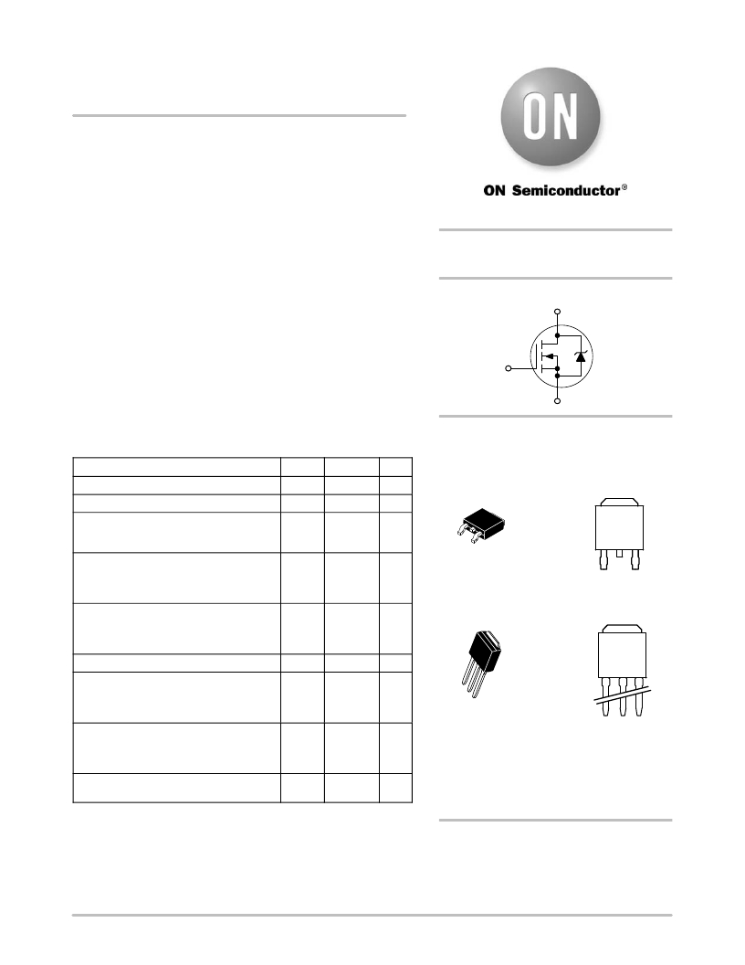
�N� ?� Channel�
�D�
�Typical� Applications�
�?� Power� Supplies�
�?� Converters�
�?� Power� Motor� Controls�
�?� Bridge� Circuits�
�G�
�S�
�MAXIMUM� RATINGS� (T� J� =� 25� °� C� unless� otherwise� noted)�
�Rating� Symbol�
�Drain� ?� to� ?� Source� Voltage� V� DSS�
�Value�
�60�
�Unit�
�Vdc�
�MARKING�
�DIAGRAMS�
�4�
�Drain�
�Drain� ?� to� ?� Gate� Voltage� (R� GS� =� 10� M� W� )�
�Gate� ?� to� ?� Source� Voltage�
�?� Continuous�
�?� Non� ?� repetitive� (t� p� v� 10� ms)�
�Drain� Current�
�?� Continuous� @� T� A� =� 25� °� C�
�?� Continuous� @� T� A� =� 100� °� C�
�?� Single� Pulse� (t� p� v� 10� m� s)�
�Total� Power� Dissipation� @� T� A� =� 25� °� C�
�Derate� above� 25� °� C�
�Total� Power� Dissipation� @� T� A� =� 25� °� C� (Note� 1)�
�Total� Power� Dissipation� @� T� A� =� 25� °� C� (Note� 2)�
�Operating� and� Storage� Temperature� Range�
�V� DGR�
�V� GS�
�V� GS�
�I� D�
�I� D�
�I� DM�
�P� D�
�T� J� ,� T� stg�
�60�
�"� 20�
�"� 30�
�9.0�
�3.0�
�27�
�28.8�
�0.19�
�2.1�
�1.5�
�?� 55� to� 175�
�Vdc�
�Vdc�
�Adc�
�Apk�
�W�
�W/� °� C�
�W�
�W�
�°� C�
�1� 2�
�3�
�4�
�DPAK�
�CASE� 369C�
�STYLE� 2�
�“SURFACE� MOUNT”�
�1�
�Gate�
�4�
�DPAK� ?� 3�
�CASE� 369D�
�STYLE� 2�
�2�
�Drain�
�4�
�Drain�
�3�
�Source�
�Single� Pulse� Drain� ?� to� ?� Source� Avalanche�
�Energy� ?� Starting� T� J� =� 25� °� C�
�(V� DD� =� 25� Vdc,� V� GS� =� 10� Vdc,�
�L� =� 1.0� mH,� I� L� (pk)� =� 7.75� A,� V� DS� =� 60� Vdc)�
�Thermal� Resistance�
�?� Junction� ?� to� ?� Case�
�?� Junction� ?� to� ?� Ambient� (Note� 1)�
�?� Junction� ?� to� ?� Ambient� (Note� 2)�
�Maximum� Lead� Temperature� for� Soldering�
�Purposes,� 1/8� ″� from� case� for� 10� seconds�
�E� AS�
�R� q� JC�
�R� q� JA�
�R� q� JA�
�T� L�
�30�
�5.2�
�71.4�
�100�
�260�
�mJ�
�°� C/W�
�°� C�
�1�
�2�
�3�
�“STRAIGHT� LEAD”�
�1� 2� 3�
�Gate� Drain� Source�
�3150� =� Device� Code�
�Y� =� Year�
�WW� =� Work� Week�
�G� =� Pb� ?� Free� Package�
�Stresses� exceeding� Maximum� Ratings� may� damage� the� device.� Maximum�
�Ratings� are� stress� ratings� only.� Functional� operation� above� the� Recommended�
�Operating� Conditions� is� not� implied.� Extended� exposure� to� stresses� above� the�
�Recommended� Operating� Conditions� may� affect� device� reliability.�
�1.� When� surface� mounted� to� an� FR4� board� using� 0.5� sq� in� pad� size.�
�2.� When� surface� mounted� to� an� FR4� board� using� minimum� recommended�
�pad� size.�
�ORDERING� INFORMATION�
�See� detailed� ordering� and� shipping� information� in� the� package�
�dimensions� section� on� page� 5� of� this� data� sheet.�
�?� Semiconductor� Components� Industries,� LLC,� 2013�
�January,� 2013� ?� Rev.� 5�
�1�
�Publication� Order� Number:�
�NTD3055� ?� 150/D�
�发布紧急采购,3分钟左右您将得到回复。
相关PDF资料
NTD3055L104
MOSFET N-CH 60V 12A DPAK
NTD3055L170-001
MOSFET N-CH 60V 9A IPAK
NTD30N02T4
MOSFET N-CH 24V 30A DPAK
NTD32N06LT4G
MOSFET N-CH 60V 32A DPAK
NTD32N06T4G
MOSFET N-CH 60V 32A DPAK
NTD3808NT4G
MOSFET N-CH 16V 12A DPAK
NTD3813NT4G
MOSFET N-CH 16V 9.6A DPAK
NTD3817NT4G
MOSFET N-CH 16V 7.6A DPAK
相关代理商/技术参数
NTD3055-150T4G
功能描述:MOSFET 60V 9A N-Channel RoHS:否 制造商:STMicroelectronics 晶体管极性:N-Channel 汲极/源极击穿电压:650 V 闸/源击穿电压:25 V 漏极连续电流:130 A 电阻汲极/源极 RDS(导通):0.014 Ohms 配置:Single 最大工作温度: 安装风格:Through Hole 封装 / 箱体:Max247 封装:Tube
NTD3055AV1
制造商:Rochester Electronics LLC 功能描述:- Bulk
NTD3055AVL1
制造商:ON Semiconductor 功能描述:
NTD3055AVT4
制造商:Rochester Electronics LLC 功能描述:- Bulk
NTD3055L
制造商:Freescale Semiconductor 功能描述:
NTD3055L104
功能描述:MOSFET 60V 12A N-Channel RoHS:否 制造商:STMicroelectronics 晶体管极性:N-Channel 汲极/源极击穿电压:650 V 闸/源击穿电压:25 V 漏极连续电流:130 A 电阻汲极/源极 RDS(导通):0.014 Ohms 配置:Single 最大工作温度: 安装风格:Through Hole 封装 / 箱体:Max247 封装:Tube
NTD3055L104/D
制造商:未知厂家 制造商全称:未知厂家 功能描述:Power MOSFET 12 Amps, 60 Volts, Logic Level
NTD3055L104-001
功能描述:MOSFET 60V 12A N-Channel RoHS:否 制造商:STMicroelectronics 晶体管极性:N-Channel 汲极/源极击穿电压:650 V 闸/源击穿电压:25 V 漏极连续电流:130 A 电阻汲极/源极 RDS(导通):0.014 Ohms 配置:Single 最大工作温度: 安装风格:Through Hole 封装 / 箱体:Max247 封装:Tube